VLSI and Integrated Circuits
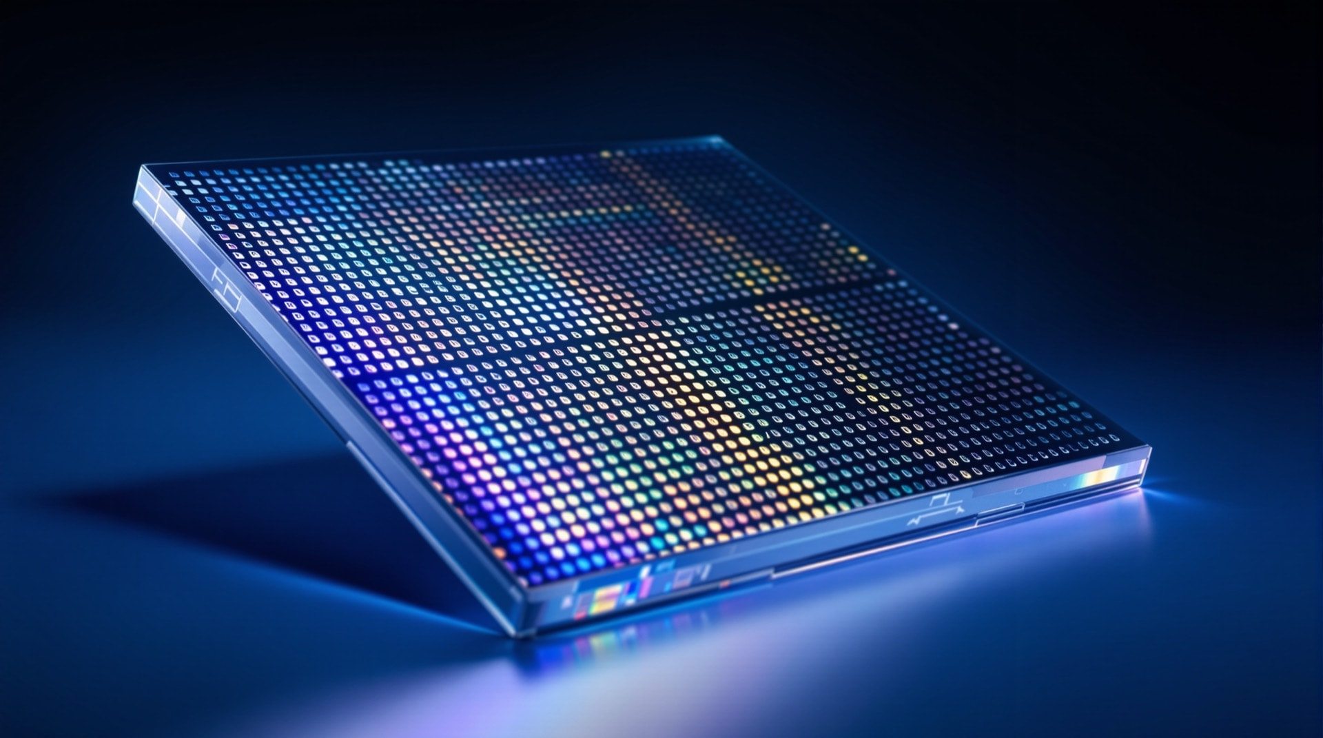
Very large scale integration is the practice of designing and manufacturing circuits containing enormous numbers of transistors on a single piece of silicon. "Enormous" has drifted upward continuously — from thousands, to millions, to tens of billions on a single die. The interesting engineering question is not how transistors work, but how any human process can produce a correct design containing tens of billions of anything.
Abstraction Is the Whole Answer
No individual understands a modern processor at transistor level, and no design methodology requires them to. The field is organised into layers, each hiding the one below behind a well-defined interface.
- Architecture — what the chip does: instruction set, memory hierarchy, functional units.
- Register transfer level — how data move between registers each clock cycle, expressed in a hardware description language. This is where most design work occurs.
- Logic — gates and flip-flops, generated automatically from RTL by synthesis tools.
- Circuit — the transistor arrangements implementing each gate, drawn from a characterised standard-cell library.
- Physical — actual placement and wiring on the die, produced by place-and-route tools.
An engineer writing RTL reasons about data flowing between registers, not about transistors. The layers below are handled by automated tools and by libraries characterised once and reused across thousands of designs. This is why chip complexity has grown far faster than design team sizes: the abstraction stack absorbs the growth. It is also why leaks in the abstraction — physical effects that force a designer to reason across layers — are so disruptive, and the important ones are discussed below.
The CMOS Transistor and Why It Won
Complementary metal-oxide-semiconductor logic pairs two transistor types so that, in either stable state, one is off and blocks current. A CMOS gate holding a steady value therefore draws almost no current. Power is consumed mainly when it switches.
That property is why CMOS displaced every competing logic family. Static power was essentially free, so more gates could be integrated without the heat becoming unmanageable.
"Essentially free" held for decades and then stopped holding. As transistors shrank, the insulating layers became thin enough that electrons tunnel through them quantum-mechanically, and thresholds fell low enough that transistors nominally off still conduct measurably. Leakage power — consumed continuously by a circuit doing nothing — became a first-order design constraint. This is the clearest example of physics puncturing an abstraction: a phenomenon belonging to device physics reached up and changed how architects design.
Power, and the End of Frequency Scaling
Dynamic power scales with capacitance, with the square of supply voltage, and linearly with clock frequency. The quadratic voltage term is the lever, and it explains a great deal of modern design.
Reducing supply voltage cuts power dramatically, but transistors switch more slowly at lower voltage, so the achievable clock frequency falls. This trade drove the industry-wide shift in the mid-2000s from raising clock speeds to adding cores: several cores at moderate voltage and frequency deliver more computation per watt than one core pushed to its thermal limit. That shift was not a preference but a consequence of the power equation, and it moved a hardware constraint directly into the domain of software, which has been adapting to it ever since.
The same reasoning produces the standard low-power techniques: clock gating stops the clock to idle blocks so they consume no dynamic power; power gating disconnects supply entirely from blocks not in use, addressing leakage as well; and dynamic voltage and frequency scaling adjusts both at run time to match demand.
Timing: The Constraint That Governs Everything
A synchronous chip works because every signal completes its journey between registers within one clock period. Verifying this is static timing analysis, and it checks two opposing conditions.
Setup violations occur when a path is too slow — data arrive after the capturing clock edge. The fix is a faster path or a slower clock.
Hold violations occur when a path is too fast — new data arrive before the register has reliably captured the previous value. Counter-intuitively, hold violations are fixed by deliberately adding delay, and unlike setup violations they cannot be resolved by slowing the clock. A chip with hold violations is broken at every speed.
These checks must hold across the full range of manufacturing variation, supply voltage and temperature, since all three affect propagation delay — which is why timing sign-off is run across multiple corners rather than at nominal conditions.
Verification Dominates the Schedule
On large designs, verification consistently consumes more effort than design. The reason is economic rather than technical: fixing a bug found in simulation costs engineering time, while fixing one found after manufacture costs a new mask set and months of schedule.
Exhaustive simulation is impossible — the state space is astronomically large — so verification relies on constrained-random stimulus guided by coverage metrics that measure which behaviours have been exercised, supplemented by formal methods that prove properties mathematically over all possible inputs rather than sampling them. Physical test after manufacture is a further discipline again, dependent on the measurement equipment able to observe signals at full speed through limited external pins.
Yield Governs Cost
Manufacturing is imperfect. Contamination and process variation mean some dies on every wafer do not work, and the fraction that do is the yield.
Because a wafer costs roughly the same regardless of how many good dies it produces, yield determines the cost per working chip almost entirely. It also explains the pressure toward smaller dies — more candidates per wafer, and a lower chance that any given one contains a defect — and the practice of binning, where partially defective parts are sold with sections disabled rather than discarded. The metrology that makes such processes controllable at these dimensions is a standing programme area at NIST, alongside its broader work in electronics.