Power Electronics
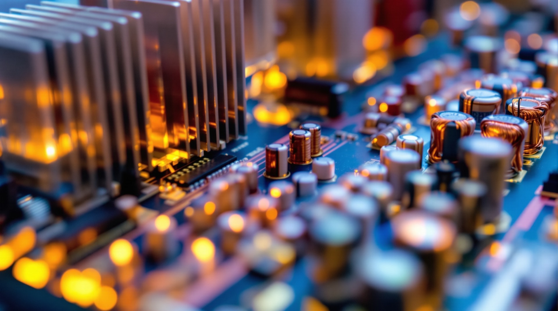
Power electronics is the discipline of converting electrical energy from one form into another — DC to AC, one voltage to another, one frequency to another — with as little of it as possible turned into heat along the way. It sits between the energy source and the load in nearly every modern system: laptop chargers, electric vehicle drivetrains, industrial motor drives, and every solar inverter feeding a grid.
The Central Trick: Switch, Do Not Resist
The foundational insight is easier to state than to appreciate. Suppose you need to turn 12 volts into 5. The obvious approach is a resistive divider, dropping the extra 7 volts across a resistance. It works, and it is terrible: the difference is dissipated as heat, so the arrangement is at best about 42% efficient, and it gets worse as the gap widens.
The power-electronic approach is to use a semiconductor switch that is either fully on or fully off, and never lingers in between. An ideal switch that is on has no voltage across it, so it dissipates nothing. An ideal switch that is off carries no current, so it also dissipates nothing. Losses occur only in the brief transitions between those states.
By switching rapidly — typically tens of kilohertz to several megahertz — and varying the fraction of time spent on, you control the average energy delivered. An inductor and capacitor then smooth that chopped waveform back into something steady. The result routinely exceeds 95% efficiency, and well-designed converters exceed 99%.
Everything else in the discipline follows from this: if losses occur mainly during transitions, then reducing losses means making transitions faster, making them less frequent, or arranging for them to happen at moments when either the voltage or the current is already near zero.
The Basic Topologies
A small number of arrangements account for most of what exists:
- Buck converter — steps a DC voltage down. The workhorse inside almost every digital device, converting a battery or supply rail to the lower voltages processors require.
- Boost converter — steps a DC voltage up, storing energy in an inductor's magnetic field and releasing it at higher potential.
- Buck-boost and derivatives — handle inputs that may be above or below the desired output, such as a battery discharging across a wide range.
- Inverter — synthesises AC from DC by switching in a pattern that approximates a sine wave, usually via pulse-width modulation. This is what connects solar arrays and battery systems to a power grid, and what drives the motor in an electric vehicle.
- Rectifier — the reverse operation, converting AC to DC. Modern active rectifiers use controlled switches rather than passive diodes, which improves both efficiency and the quality of the current drawn from the supply.
Where the Losses Actually Live
Understanding a converter's efficiency means separating two distinct loss mechanisms, because they respond to design changes in opposite directions.
Conduction losses occur while a switch is on and carrying current through a small but non-zero resistance. They scale with current and are largely independent of switching frequency.
Switching losses occur during transitions, when voltage and current are momentarily both non-zero at the same time. Each transition costs a fixed packet of energy, so these losses scale directly with switching frequency.
This produces the discipline's characteristic trade-off. Raising the switching frequency lets you use physically smaller inductors and capacitors, because each cycle moves less energy — a large benefit for size, weight and cost. But it multiplies switching losses. Every converter design is a chosen point on that curve, and the technology that moves the whole curve is what makes new device materials genuinely significant rather than merely incremental.
Why Silicon Carbide and Gallium Nitride Changed Things
For decades the switch was a silicon MOSFET or IGBT, and silicon's material properties set the boundaries. Wide-bandgap semiconductors — principally silicon carbide (SiC) and gallium nitride (GaN) — have a larger energy gap between their valence and conduction bands, and that single property cascades into several practical advantages.
They withstand much higher electric fields, so a device rated for a given voltage can be physically thinner, which lowers its on-resistance and therefore its conduction losses. They switch faster, cutting switching losses. And they tolerate higher junction temperatures, which relaxes the cooling requirements that often dominate a converter's size and cost.
The combined effect is not a few percentage points. It allows converters that are simultaneously smaller, cooler and more efficient — which is why compact fast chargers and modern EV drivetrains arrived roughly when these devices became affordable. The underlying materials science is covered in the device physics page, and the wider research programme sits within work supported by bodies such as the DOE Office of Science.
The Problem Fast Switching Creates
Faster transitions are not free. A switch that changes state in tens of nanoseconds produces very steep voltage and current edges, and steep edges are rich in high-frequency content. That energy does not stay politely inside the converter: it couples into nearby conductors, radiates from any trace acting as an unintentional antenna, and propagates back down the supply cable.
This is electromagnetic interference, and managing it is a substantial part of real converter design — layout discipline to minimise loop areas, filtering at the boundaries, careful grounding, and shielding where the rest is insufficient. It is genuinely an electromagnetics problem wearing a power-conversion hat, and it is where otherwise sound designs most often fail certification.
Verifying any of this depends on measurement equipment fast enough to see what is happening, which is not a trivial requirement at these edge rates; the instrumentation page covers why probe bandwidth and grounding technique change the answer you get. Measurement science for electronic systems is a standing programme area at NIST.